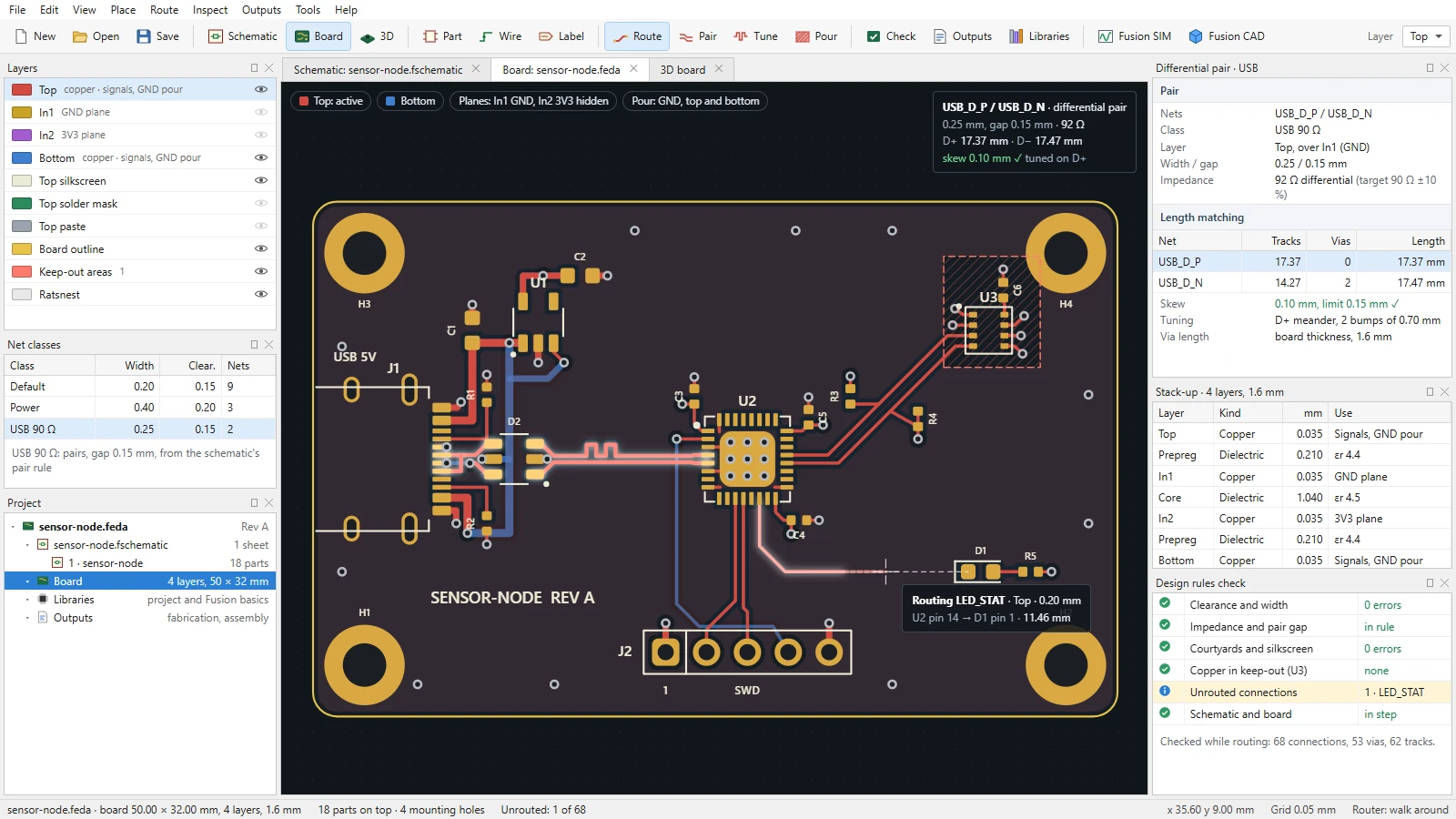
What Fusion EDA brings together.
WHAT IT ENABLES
Schematics, parts, boards, and the files that make them stay connected from the first sketch to manufacturing. Fusion EDA is in development: its schematic library, part libraries, boards, design rules check, router, and manufacturing files are being built, with a command line, a design window and a library editor drawn by Fusion 3D Engine, the rest is planned, and the screens shown are design mockups with illustrative data.
Schematic capture
01 · IN DEVELOPMENTHierarchical schematics with buses and net labels, an electrical rules check as you draw, and the bill of materials built from the schematic. The schematic library underneath, with its rules check, bill of materials, buses across sheets, and sheets used more than once, is being built now, and the development build’s window places parts, draws wires, labels, and sheets, and numbers designators, with undo.
Parts with symbol, footprint, and 3D model
02 · IN DEVELOPMENTEach part keeps its symbol, footprint, 3D model, parameters, and part number together, with every pin matched to a pad. Part libraries are being built now, with Fusion’s own common parts: resistors, capacitors, LEDs, packages, headers, and mounting holes, each with a 3D model, and a library editor for symbols, footprints, and parts.
PCB layout
03 · IN DEVELOPMENTStack-ups, design rules, placement, copper pours, and planes, with the schematic and the board kept in step in both directions. Boards that follow their schematic and a design rules check for clearances, widths, keep-outs, and unconnected nets are being built now; the development build’s window draws the board’s outline, pours, and keep-outs and edits its stack-up and rules.
Interactive routing
04 · IN DEVELOPMENTWalk-around and push-and-shove routing, differential pairs routed to a target impedance, and length tuning. The router is being built now: tracks around other nets with vias where they must change layers, other tracks and vias pushed aside on every layer, pairs routed together through vias with their impedance worked out from the stack-up, meanders to a given length with vias counted, and an autorouter for the whole board. In the development build’s window, tracks are routed by hand the same way, following the pointer.
Manufacturing outputs
05 · IN DEVELOPMENTGerber X2, Excellon drill files, IPC-2581, pick-and-place, and the bill of materials, written from the board as it is. Gerber X2 with silkscreen, drill files with a drill map, pick-and-place, and bill of materials files are being built now, with IPC-2581 valid against IPC’s schema, and panels of several boards with rails, fiducials, and v-score lines or breakaway tabs.
A 3D board view
06 · IN DEVELOPMENTThe board and its parts in 3D, drawn by Fusion 3D Engine. The development build’s window shows the board in 3D with its copper, legends, and holes, and its parts from their 3D models, and writes the board in 3D as glTF.
Designed with Fusion CAD
07 · IN DEVELOPMENTThe board’s outline, mounting holes, keep-outs, and part heights shared with Fusion CAD in both directions, so a board and its enclosure are designed together. Both directions work between the development builds of Fusion EDA and Fusion CAD: the outline, holes, and keep-outs drawn there come in, and the board and its parts go back.
One schematic with Fusion SIM
08 · IN DEVELOPMENTOne schematic editor and file format shared with Fusion SIM: a circuit tried in Fusion SIM opens in Fusion EDA as the start of a real design. The file format is agreed with Fusion SIM, and Fusion SIM’s development build already uses the library both share. Fusion EDA’s window has Fusion SIM simulate the schematic and lists what each net reads.
Board-level by design
09 · PLANNEDFusion EDA designs circuit boards and is licensed through Fusion’s license files like Fusion’s other installed products. Designing chips is not planned.